Repository navigation
SYN-363 - PT100 4-wire RTD analog front end board - #375
nyagamunene wants to merge 32 commits into
Conversation


Signed-off-by: nyagamunene <stevenyaga2014@gmail.com>
…907 3.3 V LDO

Signed-off-by: nyagamunene <stevenyaga2014@gmail.com>
Signed-off-by: nyagamunene <stevenyaga2014@gmail.com>
Signed-off-by: nyagamunene <stevenyaga2014@gmail.com>
Signed-off-by: nyagamunene <stevenyaga2014@gmail.com>
Signed-off-by: nyagamunene <stevenyaga2014@gmail.com>
Signed-off-by: nyagamunene <stevenyaga2014@gmail.com>
Rebuild the floorplan around the signal chain instead of scaling it: analog chain and input filter on the left, MCU/flash/crystal and USB on the right, connectors on the edges. The board drops from 63.1 x 51.1 mm to 50.1 x 44.1 mm.

- U2/U4 9.6 mm apart, Y1 below U2, USB-C at the top edge, SWD and PT100 at the bottom.
- R_TIE moved to the AGND/DGND bisector at (31.4, 31.5); all 54 ground pads sit on their own side of the split.
- 349 segments, 61 vias, 597.1 mm of copper, 41 nets connected, 0 open.
- KiCad DRC 0 errors / 0 warnings / 0 unconnected, ERC 0 errors / 2 library warnings, tie check R_TIE only.
- U1 label moved; 24 passive/TVS reference labels hidden where the compact layout has no clear spot (refdes remain in BOM, PnP, schematic).
- Record the all-absolute sidecar re-packing defect and refresh QUALIFICATION/SHA256SUMS.

206a380 to
5ec0166
Compare
Move J2 down 1.5 mm so both headers sit at y = 41.5 mm with their bodies 0.8 mm from the bottom edge. J2 carries no ground pads, so the AGND/DGND split and the route topology are unchanged.

Refresh the route, reports, Gerbers and renders: 339 segments, 64 vias, 586.6 mm, 41 nets, 0 open; DRC 0 errors / 0 warnings / 0 unconnected; R_TIE still the only ground tie.

Record why J1 stays at (39.5, 6.0): centering it was tried and leaves an unconnected AGND/DGND pour sliver at U2's 0.4 mm pad row that the stitching search cannot tie.
Cut a 16.4 x 20 mm notch out of the empty top-left corner, leaving the main top edge x 26.4..52.59 mm so J1 at x 39.5 is centred. The left tab keeps H1 and the top-left ground fence via, and the proven route is unchanged.

J2 and J3 stay level at y = 41.5 mm, 0.8 mm from the bottom edge.

SynthSpec has no non-rectangular outline primitive, so check.sh applies cut_outline.py after export and re-exports the Gerbers/drill from the cut board. DRC 0 errors / 0 warnings / 0 unconnected; R_TIE remains the only ground tie. Board area is 1880 mm², down from the rectangular 2208 mm² and the original 3536 mm².
Do not claim the SI/PI/RF review has not happened. The board and route review is in progress with the designated reviewer; keep the separate part-level caveat for Y1 and the three registry reviews.
Keep the parsed net number as f64 for the format lookup instead of casting it to usize, which clippy denies under -D warnings. The test still passes.
Plot F.Cu, In1.Cu, In2.Cu and B.Cu from the committed board into one labelled panel so the PR shows the 4-layer stackup and the AGND/DGND split on every layer.

Class-B qualification review — changes requestedCI is passing and the implementation is mergeable, but this is not ready to be accepted as a Class-B qualification board. Please close the following items:
The automated routing and KiCad DRC gates are useful, but they do not constitute Class-B qualification. Please address these items before approval; the acceptance criteria should not be reduced to make the PR mergeable. |
1 similar comment
Class-B qualification review — changes requestedCI is passing and the implementation is mergeable, but this is not ready to be accepted as a Class-B qualification board. Please close the following items:
The automated routing and KiCad DRC gates are useful, but they do not constitute Class-B qualification. Please address these items before approval; the acceptance criteria should not be reduced to make the PR mergeable. |
The placement sidecar now carries a closed [[outline]] in board millimetres. build_pcb uses it instead of the fitted rectangle, so the top-left notch is generated by a normal synth export-kicad.

Remove cut_outline.py and the post-export cut/re-export from check.sh; the Gerbers and drill now come from the same notched board. Add a sidecar parse/round-trip test for the outline.

Fresh export: 340 segments, 65 vias, 557.8 mm, 41 nets, 0 open; DRC 0 errors / 0 warnings / 0 unconnected; R_TIE remains the only ground tie.

|
Item 2 (reproducibility) is addressed in c08f766: the board outline is now a closed |

The 50.1 x 44.1 mm rectangle left 24 x 22 mm of bare board above the
analog chain. Move U3, C_RI, L2, C_RO, R_RST and R_CC2 into it so the
left column is populated from the top edge to J2.

The RTD input chain (J2, the RC filter, U1) is unchanged. VREF now runs
from U3 at (12, 12) to C_RV at the ADC pin; C_RV stays at REFP0.
The exported netlist embeds the absolute path of the schematic, so the
committed evidence named the machine it was built on. Generate the
netlist before the path rewrite and include it in the same pass that
already relativises release.json and the routing record.
Fresh export from e7372ca: 373 segments, 67 router vias, 664.1 mm of
copper, 40 nets, 0 open. KiCad DRC 0 errors / 0 warnings / 0
unconnected; ERC 0 errors / 2 library warnings; one GND plane.

The RTD and AIN net lengths are unchanged. VREF is 21.38 mm on F.Cu
with no via. USB total path 21.05 mm (DP) and 19.32 mm (DN), 1.73 mm
mismatch. Synth SI: 20 warnings, 18 layer changes and 2 parallel runs.

Refresh the renders, reports, netlist, SHA256SUMS and the two
documents.
GitHub moved ubuntu-latest to 26.04 between runs. The KiCad 10 PPA has
no package for 26.04, so install-kicad.sh aborts rather than fall back
to KiCad 9 and every job fails before it compiles anything. Pin the
image the artifact checks were proven against.


What type of PR is this?
A design, placement and routing contribution for the SYN-363 Class B qualification board. It is not a qualification result. The board is routed with FreeRouting and passes KiCad's DRC, and the SI/PI/RF review is with the designated reviewer. It has not been fabricated or tested on hardware, and Class-B sign-off (#361) is not claimed here.
The branch is the Class B board branch, so it also carries the prerequisite commits from this work: #362 (ADS124S08 and REF5025 registry parts,
612ccc4), #364 (BLE node parts,d17e651, not this board), and #363's split-ground fence-via fix (81bb62a). The BLE environment node board itself is not in this PR. The branch also includes a merge ofmain; the merge conflicts were resolved by hand.This revision reworks the ground to one GND plane on all four layers. The earlier split-ground board left two isolated DGND pours on the merged router; the single plane removes that failure mode and the R_TIE part. The notch is gone: the board is a plain 50.1 x 44.1 mm rectangle (2209 mm²) with a rectangular
[[outline]], so a normalsynth export-kicadneeds no post-export cut. J1 stays at its proven top-edge position because centering it fragmented U2 ground escape. One via-in-pad at C_DV.2 keeps the tighter outline clean; the source declaresrequires via_in_padand the profile isjlc-filled-via. It also re-places the reference and analog-supply support into what was a 19 x 19 mm bare rectangle in the top-left; the RTD input chain is unchanged.What does this do?
A 4-wire PT100 measurement front end with a USB-C readout:
.synthsource isqualification/class-b/rtd-afe/rtd_afe.synth; every part has a position inrtd_afe.placement.layout.toml(board millimetres). The schematic has no sidecar.Files
All in
qualification/class-b/rtd-afe/:rtd_afe.synth: the board sourcertd_afe.placement.layout.toml: board millimetres, every part has a position, the label overridescheck.sh: exports and autoroutes, runs KiCad DRC/ERC on the result, renders the images, asserts the single GND plane in pcbnew, and stamps the source revisionREADME.md: what the board is, the filter and ground reasoning, the routing numbers, the known limitsQUALIFICATION.md: the check results, the per-part datasheet table, the single-ground argument, the mechanical geometry table, the open review items, the Synth defectskicad/: the routed.kicad_pcb, schematic, symbol library, project, DRC rules, BOM, PnP, Gerbers and drill filesreports/:release.json, the delivered DRC and ERC reports, the KiCad netlist, the FreeRouting record and the connectivity reportimages/: 3D top, bottom and angled views and the schematicSHA256SUMS: hashes of the committed artifactsExporter changes in this PR:
crates/synth-kicad/src/pcb.rs: per-instance footprint UUIDs and outline-aware ground fence vias.crates/synth-router/src/island_vias.rs: ground-return via selection and island repair.crates/synth-router/src/lib.rs: an untied island still blocks; a missing return via is the existingW-SYNTH-DRC-016advisory.crates/synth-kicad/src/bom.rs: BOM now carriesdielectric,voltage,toleranceandpowerfrom the source.crates/synth-cli/src/release.rs:source_revisionis stamped fromSYNTH_SOURCE_REVISION, andinputis checkout-relative.Pictures
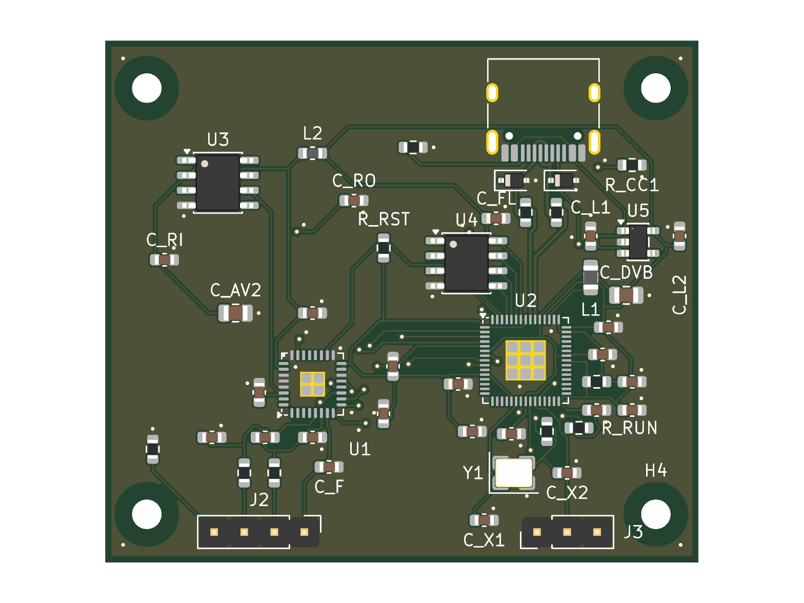
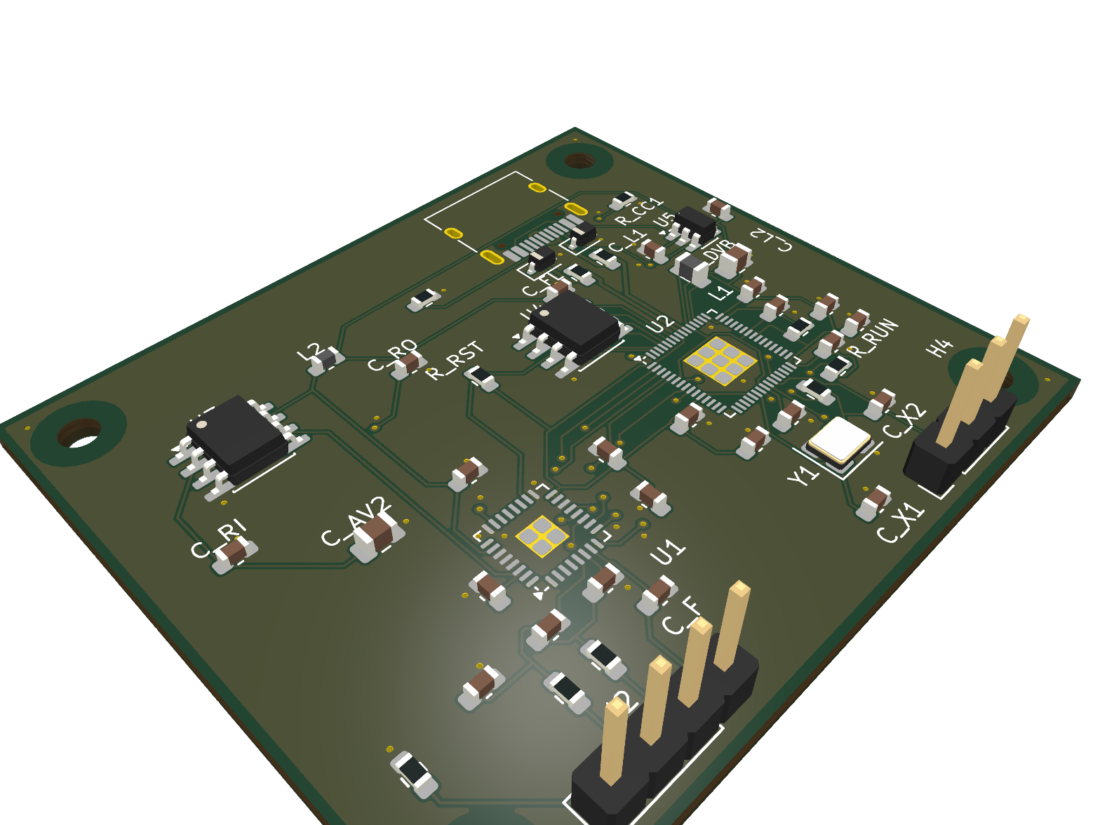
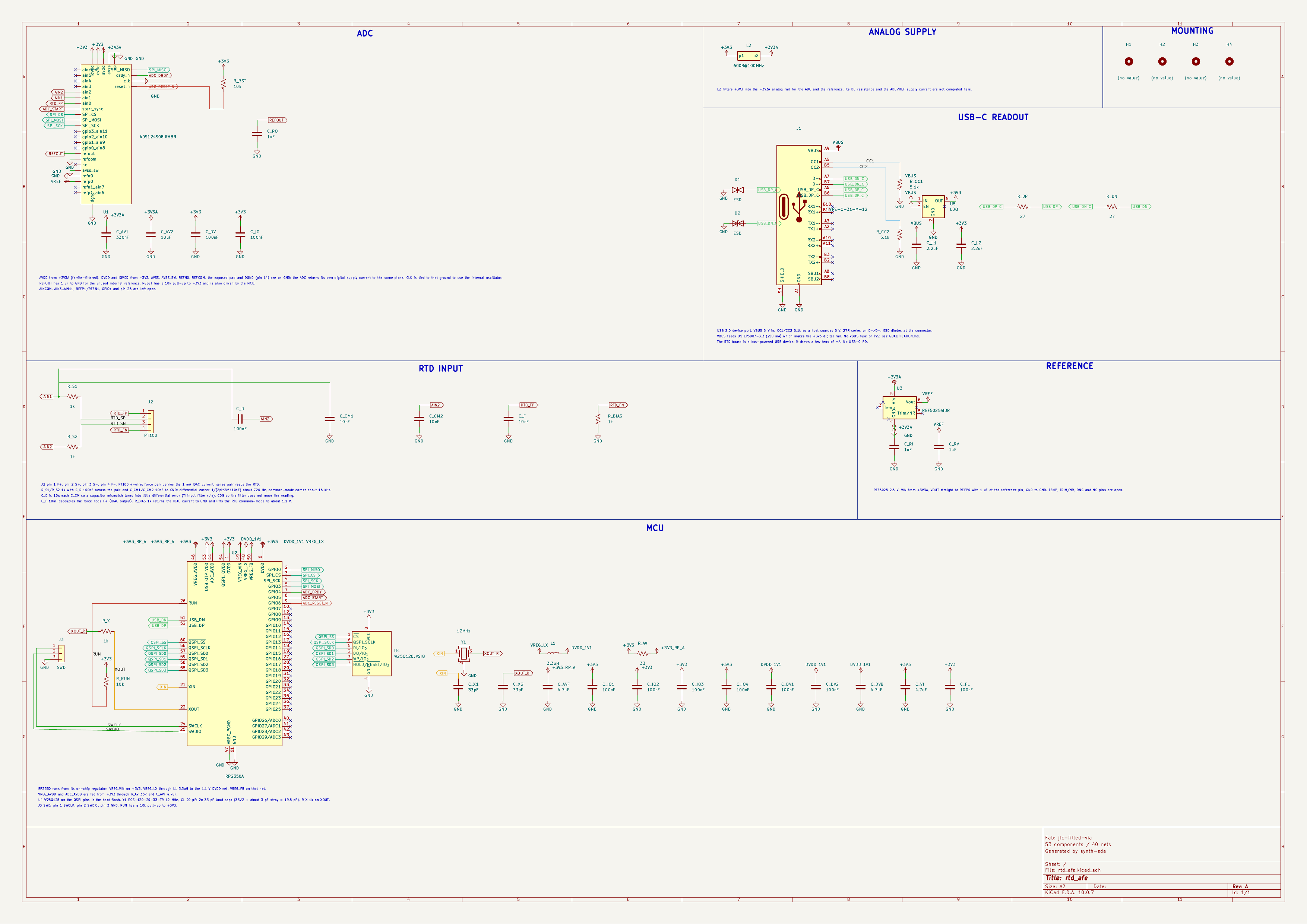
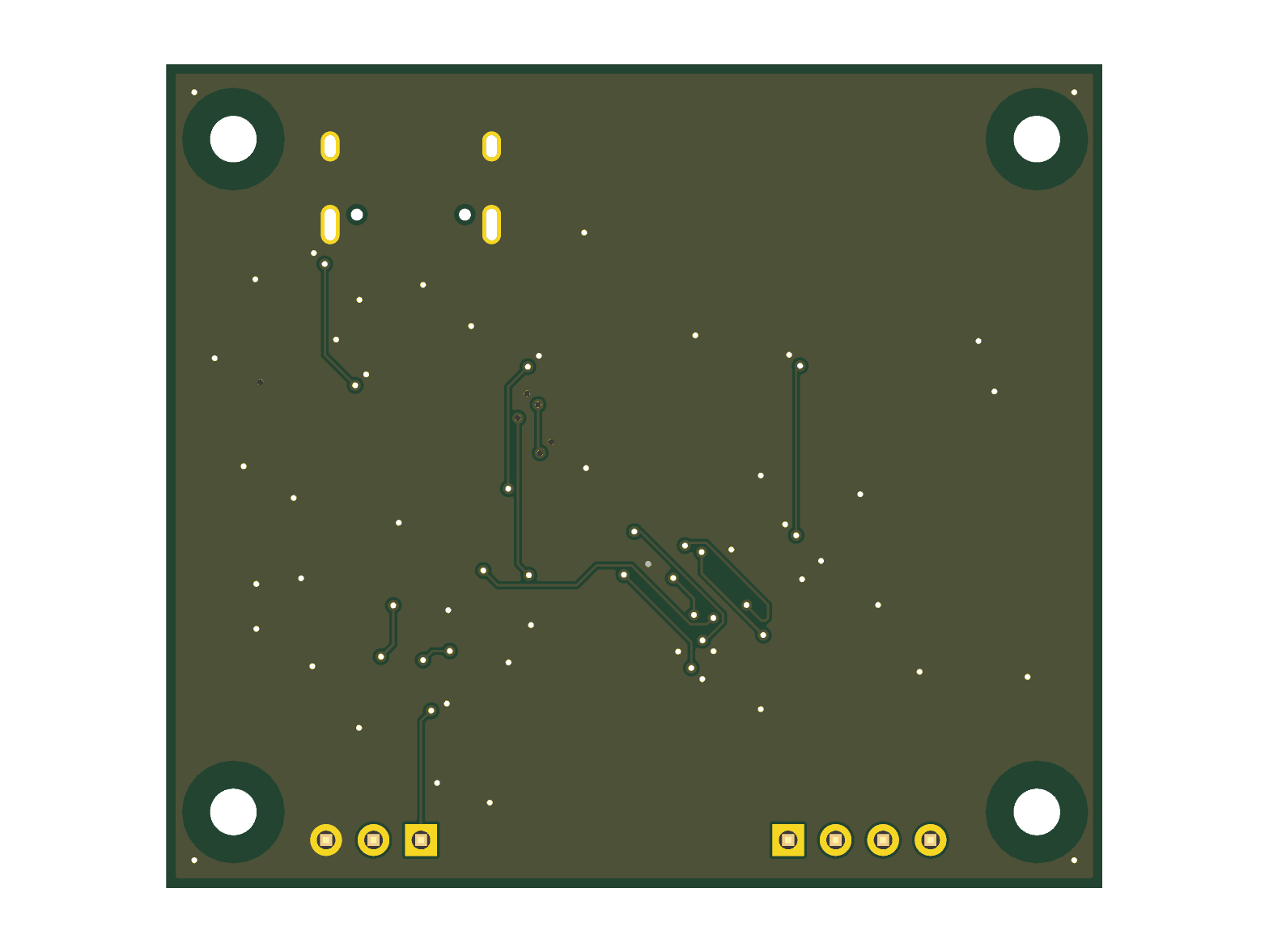
Rendered with
kicad-clifrom commit51104b2.3D top view:
3D angled view:
Schematic:
3D bottom view:
State of the board
Routed with FreeRouting 2.4.1 on Java 25, KiCad 10.0.7, Synth
synth-cli 0.1.1. The reports are from the run recorded inreports/release.json;source_revisionnow names the commit that produced the package andinputis checkout-relative.check.shasserts that with pcbnew.kicad-cli pcb drc --severity-all --refill-zones: 0 errors, 0 warnings, 0unconnected_items.pcbnew.LoadBoardreopens the board. Synth's connectivity report also has 0 open nets.Device:Ferrite_Beadis the old library name (KiCad 10 hasDevice:FerriteBead), and the embedded REF5025ID symbol differs from the installed library copy. Both are drawing/library comparisons; the netlist and PCB parity are clean.synth validate: no errors. The warnings and their dispositions are listed inQUALIFICATION.md.release.jsonkeepsproduction_status: untrustedandrelease_ready: falsebecause the 12 MHz crystal part has no part-level reviewer (the--allow-unverified-partsoverride). That is not a DRC failure and not a fabrication approval.QUALIFICATION.md: the mounting holes leave 2.25 to 2.83 mm of material, and the tab, connector fit and enclosure clearance remain unverified.Review comments
Fixed:
[[outline]], so a normalsynth export-kicadproduces the PCB, Gerbers and drill directly with no post-export cut.bom.csvnow hasdielectric,voltage,toleranceandpowercolumns copied from the structured.synthattributes. The C0G filter caps and 0.1% resistors are visible to an assembler; regression teststructured_attributes_get_their_own_columns.release.jsonstampssource_revisionfrom the checked-out commit and records a checkout-relativeinputpath;check.shalso relativises the netlist path, soreports/rtd_afe.netno longer names the build machine.QUALIFICATION.mdhas a measured mechanical geometry table for the holes, tab and connectors; the unverified fit items are named there.ensure_body_uuidsnow derives ids per placed instance and replaces stock ones; the regression test is included.W-SYNTH-DRC-016SI warnings, while an untied copper island still blocks and is reported.ci.ymlpinsubuntu-24.04.ubuntu-latestmoved to 26.04 on 2026-11-03, where the KiCad 10 PPA has no package, so every job failed in the KiCad install step before compiling anything.Open, recorded as qualification limitations:
Not verified